Kicad schematic for opamp based preamp circuit used with my adc_interface project
I designed this circuit to use with interfacing with my De0 Nano's onboard analog to digital circuit (ADC). The cicuit has the following features
- 0-50 x Gain
- Bandwidth (didnt really calculate, but designed for use with audio)
- Amp requires 12-20V DC supply
- Vout level protection circuit requires 3.3V DC supply
- 12V rail is provided by 8 1.5V batteries
- 3.3V rail to protection clamping diodes connect to: * GPIO-1 - pin 29 (VCC3P3) * GPIO-1 - pin 30 (GND)
- Vout connected to: * GPIO-3 - pin 24 (Analog_In0)
The compontents have not been chosen to be the best for the job. These (i.e. the uA741CP and diodes) were what I had available in my parts bin, many of which I pulled off of old PCB's. In the future I would like to revise. But this circuit gets the job done for cheap.
The circuit can be analysed broken into 3 main parts:
- Microphone Biasing (left of C1)
- Non-Interting Op-amp (between C1 and C3)
- Output Biasing and Clamping (right of C3)
The capacitors between each part are coupling capacitors which are used to allow ac signals to pass through each stage.
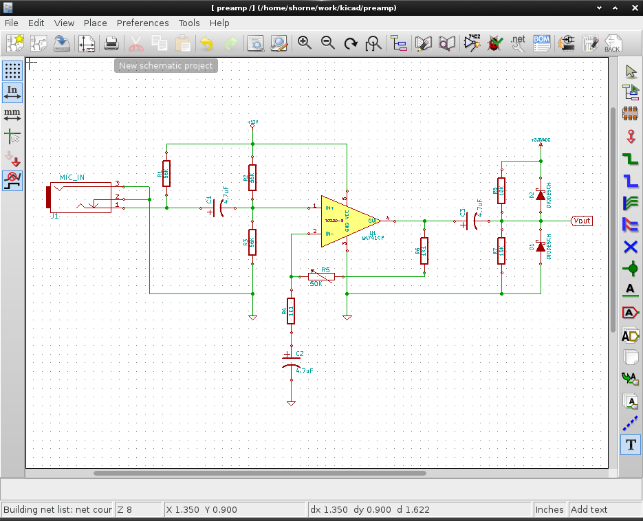
Most microphones need to be biased with a voltage and a large resistor. You can think of a microphone as a capacitor, when the capacitor plates move with respect to eachother the capacitance change causing a voltage change. The ouput voltage of a typical microphone will be rated in dB from the manufacturer, around -40dB. The microphone I am using outputs a signal of about 20mV.
The Non-Interting Op-Amp circuit is a typical op-amp pattern but it contains two simple tricks that they dont often teach you in your op-amp theory courses. If you look at most op-amp circuits they will have a relatively high negative and positive rail for powering the op-amp. For portable devices this is not practical and we need way to power the device with a single supply.
The single supply circuit is supported by the components R2, R3 and C2. Also note, by using coupling capacitors C1 and C3 on each side of the Op-amp circuit the DC (supply) components are isolated from other supplies. R2 and R3 create a voltage divider network allowing the op-amp IN+ voltage to sit at half the supply voldage 6V (kind of a virtual ground). Next C2 is also needed to allow IN- to rest at 6V (the virtual ground). This means at rest there is no current flowing through the feedback loop or down to ground.
Note: If C2 was shorted we would would have a path for 6V DC to go to ground and that would not work.
Next, in order to make sure our ouput does not cause any damage to the final consumer of the signal we add output clamping or clipping. This circuit is designed to feed into a ADC chip expecting a signal between 0 and 3.3 volts.
The components R7 and R8 create voltage divider to bias the output at half 3.3V. This allows Vout normally sit at 1.65V and input charnges will cause the Vout to go above or below 1.65V like negative and positive voltages of an audio signal.
The diodes D1 and D2 are clamping diodes. If the output voltage goes above 3.3v the D2 diode will conduct and the output will essentially get clamped to 3.3V. If the voltage goes below 0V then D1 will activate and the ouptut will be clamped to 0V. At the rest voltage ~1.6V neither diode is active and the output is 1.6V.
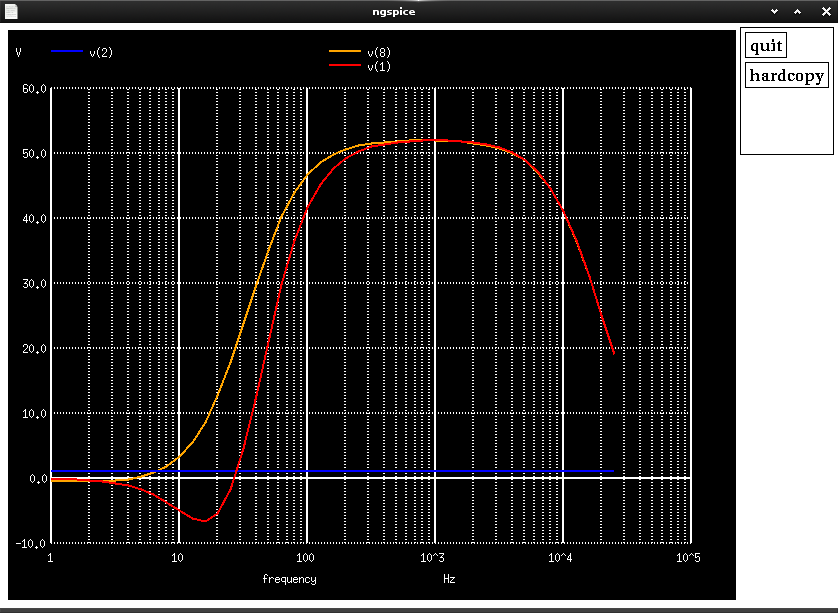
I took some time to simulate the performance of the circuit in ngspice. The bandwidth of the circuit is about 100hz to 10Khz. This is ideal for simple voice amplification as I require but not good for high end audio.
In the below waveforms the voltages plotted are as follows:
- V(2) - input voltage, 20mV 440hz sine wave
- V(8) - voltage output of op amp
- V(1) - voltage output after clamping stage with a 2k load

- Currently this uses a chip
uA741CPchip which requires a12Vsupply. Switch it out for something that can run on3.3Vand power the entire circuit off3.3V.